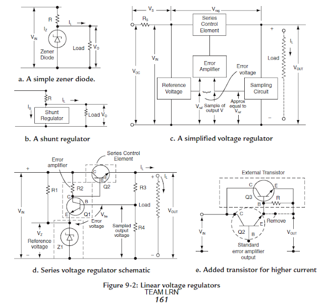
The shunt regulator shown in Figure 9-2b also shunts current from the load but is designed to handle much larger currents. It duplicates the zener diode regulator. Initially, IS is a maximum through the shunt. As IL increases to a maximum, IS will decrease to a minimum. It is packaged to handle much greater power dissipation, since the device power dissipation is VO times IS. Linear Series Voltage Regulators A true feedback-type linear voltage regulator is shown in Figure 9-2c. All components operate in their linear mode. It is a simplified block diagram that does not have all the bells and whistles that are designed into IC regulators today, but the modern IC regulators are based on the same principles. The input voltage, a DC voltage, is separated from the load by a control element in series between VIN and VOUT. There is a voltage drop across the control element of VREG. The series control element is controlled by an error amplifier.
The error amplifier amplifies a voltage difference, called the error voltage, between a reference voltage and a sampled portion of the output voltage approximately equal to the reference voltage. Changes in the load current cause VOUT to vary and the error voltage to change such that the series drop across the control element compensates for the change in VOUT.
Load Variations
The regulation works as follows: If IL increases it will tend to reduce Vout. The reduction in VOUT is fed through the sampling circuit to an input of the error amplifier. The reference voltage is on the other input. Since the reference voltage is constant, the error voltage decreases and causes the voltage across the control element to decrease. As a result, Vout increases to compensate for the initial decrease. Likewise, if IL decreases, it tends to increase Vout. Increasing Vout increases the error voltage, which increases the control element voltage, Vreg and reduces Vout to compensate for the initial increase. The stable operating point of the system is such that with Vin a particular value and Vout a specified value, the error voltage is tending toward zero.
Actual Linear Voltage Regulator Circuit
Figure 9-2d is a schematic of the interconnection of components for a linear series voltage regulator. The active devices shown are bipolar transistors, but MOS devices can (and are) used for the same design. NPN transistors and a positive output voltage are used in the design because the circuit is a bit easier to understand. Note first that the series control element is just a NPN transistor. Note also that the reference voltage is really the zener voltage regulator that was discussed in Figure 9-2a. The only variations in the zener diode current will be those caused by variations in the input voltage, VIN. Q1 and R2 form an inverting amplifier whose output drives the base of Q2, the series control element. The input to the amplifier is the error voltage, Vbe of Q1. The sampled output voltage under the quiescent state is equal to a Vbe voltage above VZ, the reference voltage.
Load Variations
The regulation proceeds as follows: When IL increases and VOUT tends to reduce due to the increased drop across Q2, the Vbe error voltage on Q1 reduces, reducing current through Q1 and R2. The rise in the collector voltage of Q1 and base voltage of Q2 raises the emitter voltage of Q2, increasing VOUT to compensate for the initial reduction. Likewise, for a decrease in IL, VOUT tends to increase because of the decreased drop across Q2. The Vbe error voltage increases, which reduces the Q1 collector voltage and base voltage of Q2, which reduces the emitter voltage to compensate for the initial rise in VOUT.
Line Variations
Similar regulation occurs for VIN variations. If VIN increases, VOUT tends to increase, but the reference voltage, VZ, changes very little. The error voltage increases because of an increase in VOUT, which reduces the Q1 collector voltage and base voltage of Q2, which reduces the emitter voltage, VOUT, to compensate for the increase. Similar to load variations, a decrease in VIN will be met with a compensating increase in VOUT to complete the regulation.
Higher-Current Regulators
In order to handle larger currents and, thus, more power dissipation for the regulator, external devices can be connected as shown in Figure 9-2e. Many IC regulators have the connections for the external devices provided in the design. Again, bipolar devices are used in the example, but MOS devices can be used just as well. Power devices with external heat sinks are usually required in order to satisfy the power dissipation requirements and keep the operating temperatures of the devices within specifications.


No comments:
Post a Comment